SERIES 50 HOLLOW CATHODE
SERIES 50
HOLLOW CATHODE
The Series 50 is one of our most popular hollow cathode plasma sources. It is commonly used for ALD, but also for oxidation and PECVD applications.

UHV SERIES
HOLLOW CATHODE
The Series 50 is one of our most popular hollow cathode plasma sources. It is commonly used for ALD, but also for oxidation and PECVD applications.

LARGE AREA
HOLLOW CATHODE
SOURCES
Meaglow has successfully developed and implemented designs for larger area hollow cathodes.

HOLLOW
CATHODE
FOR THERMAL
ALD SYSTEMS
Meaglow has developed a number of solutions to economically convert thermal ALD systems to plasma assisted ALD.

ALD / CVD
RESEARCH
REACTOR
Based on Meaglow’s Patented Breakthroughs in ALD Plasma Technology and CVD Pulse Deposition.

SERIES 16 HOLLOW CATHODE
The Series 16 MINI PLASMA SOURCE is the result of a mini plasma source developed for NASA Goddard.

Meaglow Ltd offers a range of hollow cathode plasma sources for the semiconductor industry. In particular the Atomic Layer Deposition (ALD) sector.
Hollow cathode plasma technology is the ‘go to’ solution for high quality nitride layers. Meaglow’s hollow cathode plasma sources offer substantial reduction in oxygen contamination (see our company white paper).
(Go to here for plasma source brochures)
Most Commonly our customers require custom solutions, so many of our plasma sources are made to order. The brochures indicated in the above link provide some guidance as to what is possible, though we would strongly suggest you contact us to address your individual requirements.
There are some standard Meaglow hollow cathode plasma source offerings. The series 50 is one of our most popular sources, and is mounted on an NW-50 flange (though the equivalent conflat arrangement is also available). See the link here.
Conversions of existing systems is also possible, and we provide some white papers for the more common conversions that we have performed. See the link here.
To date the largest source developed by Meaglow was for a 12″, 3000 watt system, though we have consulted for larger systems
Why is the hollow cathode source being adopted by the ALD sector?
Hollow Cathode Plasma Sources – addressing a paradigm shift in semiconductor industry.
- For more than 30 years, nothing much changed regarding plasma sources. Historically, for deposition purposes, plasma sources were most heavily used for PECVD (plasma enhanced CVD) and PVD (physical vapour deposition) applications. PECVD predominantly involved the deposition of the traditional materials silicon nitride, silicon oxide and amorphous silicon. For well over 30 years there was very little variation from these materials, or the means of deposition.
- A paradigm shift, nanomaterials and new methods. Inductively coupled plasmas (ICP) and capacitively couple plasmas (CCP) were the two main types used, though microwave plasmas also saw some use. However, in recent years Moore’s law has dictated a change. There has been a move to nanoscale dimensions and to new materials not historically used in the silicon industry. For instance, copper, hafnium nitride, platinum, aluminium oxide, tantalum nitride, ITO, new interconnect materials, and new dielectric materials, just to name a few.
- ALD Emerges. Since 2008 ALD has emerged as a major means of controlled thin film deposition, and now holds about 8% of the film deposition equipment market with a predicted CAGR of 15% for the period from 2012 to 2017. Right now the ALD market is ~US$500,000,000 according to a 2013 Berenberg Equity, Semiconductor Equipment Study.
Problems emerge: The old traditional solutions of CCP and ICP are being applied to ALD, but are inadequate for depositing many of the new materials now being used. There are problems with –
- Poor crystallinity
- Oxygen contamination from the plasma source (ICP sources)
- Low growth rates
- Scaling issues
For the traditional materials deposited by PECVD, i.e. silicon nitride and silicon dioxide, oxygen contamination from ICP plasma sources was not an issue. In the case of silicon nitride only the dielectric properties were of interest, in the case of silicon dioxide, oxygen was part of the material. Hence there was no reason to move to other solutions. However with the new materials, these are issues to be solved.
A different plasma source: Hollow cathode plasma sources, are an alternative to ICP and CCP sources. They’ve been around for quite a number of years and have been adopted for cathodic sputtering in PV systems, but past designs have been overly complicated for many PECVD applications involving the traditional material sets.
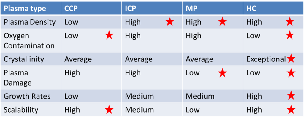
HC = hollow cathode plasma sources, MP = microwave plasma sources, ICP = inductively couple plasma sources, CCP = capacitively couple plasma sources
The Meaglow solution: With the new industry paradigm – the advent of ALD and newer materials – better solutions are required. Meaglow Ltd has developed a set of simple designs that have allowed the successful adoption of hollow cathode plasma sources in ALD systems, overcoming some of the limitations of the old technologies. The Meaglow solution is enabling the Next Generation of equipment solutions.
Although it was initially adopted because of the lower oxygen contamination seen in nitride materials, advantages of the HC plasma sources for other materials, including oxides, soon became evident. Higher growth rates and lower plasma damage levels being evident, but the simple design of Meaglow’s HC systems also make these a very cost effective alternative.
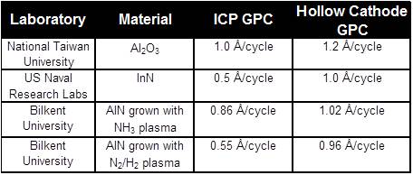
The table below shows some ALD results for direct replacement of an ICP plasma source with an HC plasma source. The greater GPC (growth per cycle) value is due to lower plasma damage, lower oxygen contamination or a combination of the two, depending on the material.
Growth per Cycle Improvement for ALD Plasma Deposition